Author Affiliations
Abstract
1 Key Laboratory of Nanodevices and Applications, Suzhou Institute of Nano-tech and Nano-Bionics, Chinese Academy of Sciences, Suzhou 215123, China
2 School of Physical Science and Technology, ShanghaiTech University, Shanghai 201210, China
3 Shanghai Advanced Research Institute, Chinese Academy of Sciences, Shanghai 201210, China
4 University of Chinese Academy of Sciences, Beijing 100049, China
A new kind of step-flow growth mode is proposed, which adopts sidewall as step source on patterned GaN substrate. The terrace width of steps originated from the sidewall was found to change with the growth temperature and ammonia flux. The growth mechanism is explained and simulated based on step motion model. This work helps better understand the behaviors of step advancement and puts forward a method of precisely modulating atomic steps.
step-flow growth GaN terrace width step motion Journal of Semiconductors
2024, 45(2): 022501

Siyi Huang 1,2,3Masao Ikeda 2,3,*Minglong Zhang 1,2,3Jianjun Zhu 2,3Jianping Liu 1,2,3,**
Author Affiliations
Abstract
1 School of Nano-Tech and Nano-Bionics, University of Science and Technology of China, Hefei 230026, China
2 Suzhou Institute of Nano-Tech and Nano-Bionics, Chinese Academy of Sciences, Suzhou 215123, China
3 Key Laboratory of Nanodevices and Applications, Chinese Academy of Sciences, Suzhou 215123, China
A suitable contacting scheme for p-(Al)GaN facilitating quick feedback and accurate measurements is proposed in this study. 22 nm p+-GaN followed by 2 nm p-In0.2Ga0.8N was grown on p-type layers by metal-organic chemical vapor deposition. Samples were then cut into squares after annealing and contact electrodes using In balls were put at the corners of the squares. Good linearity between all the electrodes was confirmed inI–V curves during Hall measurements even with In metal. Serval samples taken from the same wafer showed small standard deviation of ~ 4% for resistivity, Hall mobility and hole concentration. The influence of contact layer on the electrical characteristics of bulk p-type layers was then investigated by step etching technique using inductively coupled plasma etching and subsequent Hall-effect measurements. Identical values could be obtained consistently when a 28 nm non-conductive layer thickness at the surface was taken into account. Therefore, the procedures for evaluating the electrical properties of GaN-based p-type layers just using In balls proposed in this study are shown to be quick and useful as for the other conventional III–V materials.
GaN electrical properties ohmic contact Journal of Semiconductors
2023, 44(5): 052802

Author Affiliations
Abstract
1 School of Nano-Tech and Nano-Bionics, University of Science and Technology of China, Hefei 230026, China
2 Suzhou Institute of Nano-Tech and Nano-Bionics, Chinese Academy of Sciences, Suzhou 215123, China
Specific contact resistance to p-GaN was measured for various structures of Ni/Pd-based metals and thin (20–30 nm thick) p-InGaN/p+-GaN contacting layers. The effects of surface chemical treatment and annealing temperature were examined. The optimal annealing temperature was determined to be 550 °C, above which the sheet resistance of the samples degraded considerably, suggesting that undesirable alloying had occurred. Pd-containing metal showed ~35% lower compared to that of single Ni. Very thin (2–3.5 nm thick) p-InGaN contacting layers grown on 20–25 nm thick p+-GaN layers exhibited one to two orders of magnitude smaller values of compared to that of p+-GaN without p-InGaN. The current density dependence of , which is indicative of nonlinearity in current-voltage relation, was also examined. The lowest achieved through this study was 4.9 × 10⁻⁵ Ω·cm2 @J = 3.4 kA/cm2.Specific contact resistance to p-GaN was measured for various structures of Ni/Pd-based metals and thin (20–30 nm thick) p-InGaN/p+-GaN contacting layers. The effects of surface chemical treatment and annealing temperature were examined. The optimal annealing temperature was determined to be 550 °C, above which the sheet resistance of the samples degraded considerably, suggesting that undesirable alloying had occurred. Pd-containing metal showed ~35% lower compared to that of single Ni. Very thin (2–3.5 nm thick) p-InGaN contacting layers grown on 20–25 nm thick p+-GaN layers exhibited one to two orders of magnitude smaller values of compared to that of p+-GaN without p-InGaN. The current density dependence of , which is indicative of nonlinearity in current-voltage relation, was also examined. The lowest achieved through this study was 4.9 × 10⁻⁵ Ω·cm2 @J = 3.4 kA/cm2.
Journal of Semiconductors
2022, 43(9): 092803

Lingrong Jiang 1,2,3Jianping Liu 1,2,3,*Lei Hu 1,2,3Liqun Zhang 1,3[ ... ]Hui Yang 1,2,3
Author Affiliations
Abstract
1 Suzhou Institute of Nano-tech and Nano-bionics, Chinese Academy of Sciences, Suzhou 215123, China
2 School of Nano-tech and Nano-bionics, University of Science and Technology of China, Hefei 230026, China
3 Key Laboratory of Nanodevices and Applications, Chinese Academy of Sciences, Suzhou 215123, China
4 Nano Science and Technology Institute, University of Science and Technology of China, Hefei 230026, China
Absorption induced by activated magnesium (Mg) in a p-type layer contributes considerable optical internal loss in GaN-based laser diodes (LDs). An LD structure with a distributed polarization doping (DPD) p-cladding layer (CL) without intentional Mg doping was designed and fabricated. The influence of the anti-waveguide structure on optical confinement was studied by optical simulation. The threshold current density, slope efficiency of LDs with DPD p-CL, and Mg-doped CL, respectively, were compared. It was found that LDs with DPD p-CL showed lower threshold current density but reduced slope efficiency, which were caused by decreasing internal loss and hole injection, respectively.
polarization doping internal loss GaN laser diode Chinese Optics Letters
2021, 19(12): 121404
1 中国科学技术大学纳米技术与纳米仿生学院,合肥 230026
2 中国科学院苏州纳米技术与纳米仿生研究所,纳米器件与应用重点实验室,苏州 215123
氮化镓(GaN)基蓝光和绿光激光器在投影显示、激光加工、激光照明、存储等领域具有重要的应用前景与广泛的市场需求。本文着重介绍了GaN基蓝光和绿光边发射激光器的技术难点和相应的解决方案。在GaN基蓝光与绿光激光器中,就制备高质量InGaN/GaN多量子阱、减少内部光学损耗、增加空穴注入效率等方面分别介绍了一些结构与工艺方面的优化方法。简要介绍了垂直腔面发射激光器(VCSEL)、分布式反馈激光器(DFB)的研究现状。
半导体激光器 氮化镓 热退化 In偏析 内部光学损耗 载流子注入效率 semiconductor laser diode GaN thermal degradation In segregation internal optical loss carrier injection
Author Affiliations
Abstract
1 School of Nano Technology and Nano Bionics, University of Science and Technology of China, Hefei 230026, China
2 Suzhou Institute of Nano-Tech and Nano-Bionics, Chinese Academy of Science, Suzhou 215123, China
3 Key Laboratory of Nanodevices and Applications, Chinese of Academy of Science, Suzhou 215123, China
4 Vacuum Interconnected Nanotech Workstation (NANO-X), Suzhou Institute of Nano-Tech and Nano-Bionics, Chinese Academy of Sciences, Suzhou 215123, China
The inhomogeneous broadening parameter and the internal loss of green LDs are determined by experiments and theoretical fitting. It is found that the inhomogeneous broadening plays an important role on the threshold current density of green LDs. The green LD with large inhomogeneous broadening even cannot lase. Therefore, reducing inhomogeneous broadening is a key issue to improve the performance of green LDs.
Journal of Semiconductors
2019, 40(5): 052802
Author Affiliations
Abstract
1 Key Laboratory of Nano-Devices and Applications, Suzhou Institute of Nano-Tech and Nano-Bionics, Chinese Academy of Sciences, Suzhou 215123, China
2 University of Science and Technology Beijing, Beijing 100083, China
3 Suzhou Institute of Nano-Tech and Nano-Bionics, Chinese Academy of Sciences, Nanchang 330200, China
4 School of Nano Technology and Nano Bionics, University of Science and Technology of China, Hefei 230026, China
5 e-mail: mxfeng2011@sinano.ac.cn
6 e-mail: qsun2011@sinano.ac.cn
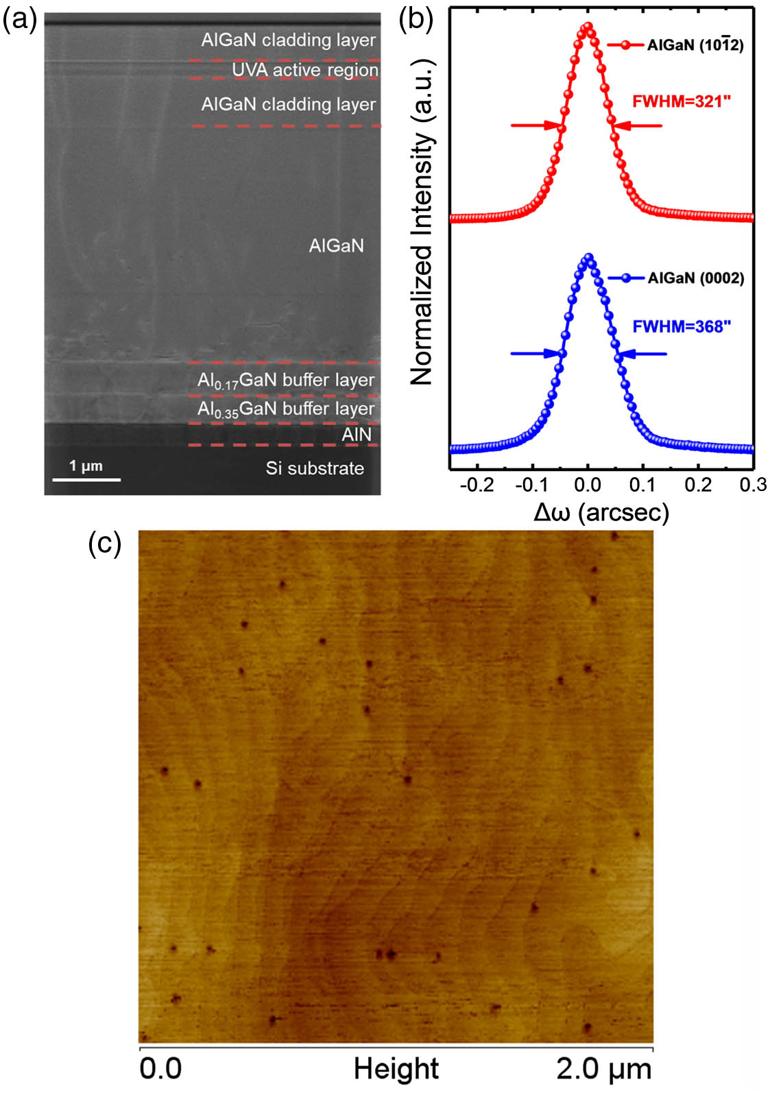
This work reports a demonstration of electrically injected GaN-based near-ultraviolet microdisk laser diodes with a lasing wavelength of 386.3?nm at room temperature. The crack-free laser structure was epitaxially grown on Si substrates using an Al-composed down-graded AlN/AlGaN multilayer buffer to mitigate the mismatches in the lattice constant and coefficient of thermal expansion, and processed into “sandwich-like” microdisk structures with a radius of 12?μm. Air-bridge electrodes were successfully fabricated to enable the device electrical characterization. The electrically pumped lasing of the as-fabricated microdisk laser diodes was evidenced by the rapid narrowing down of electroluminescence spectra and dramatic increase in the light output power, as the current exceeded the threshold of 248?mA.
Photonics Research
2019, 7(6): 06000B32


